
ATLAS e-News
23 February 2011
The ATLAS tracker upgrade: Silicon detectors for the sLHC
25 January 2011
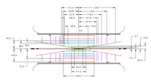
Schematic of the baseline tracker layout for the upgrade. The baseline technology is based on p-type silicon sensors ('n-in-p'), which have the advantage that they can be operated partially depleted after irradiation. A good understanding of this technology has already been achieved.
I think we all agree that 2010 was a very good year for ATLAS. The LHC ran better than expected, our detectors performed brilliantly, and quality physics papers are being churned out at an impressive rate. For 2013 and beyond we are looking forward to collision energies at 14 TeV and luminosities reaching 1034 cm-2s-1.
Given all this, it may seem strange to be planning already for a major luminosity upgrade. Shouldn't we be focusing on the current ATLAS physics programme and worry about the next steps once we have a better understanding of the physics at the LHC? The problem is it takes a long time to design, develop and build the complex detector systems we need to do physics in modern hadron collider experiments. Think of ATLAS it took 16 years from the publication of our Letter of Intent to readiness in the cavern! This is especially true for the Inner Detector upgrade, for which existing technology simply doesn't exist and new solutions have to be found.
The goal of the sLHC is to increase the integrated luminosity delivered to the experiments for physics analysis by an order of magnitude from 300 to 3000 inverse femtobarns. This will extend the physics reach of ATLAS significantly, but it also means operating in an even more challenging environment. For example, the increased collision rates will lead to higher radiation backgrounds, causing damage to detectors and electronics. The number of collisions per bunch crossing will also increase dramatically, leading to more hits in the detectors and more complex challenges for track and vertex reconstruction. Many parts of ATLAS will need upgrading, but in this article we focus on the inner tracker.
The current ATLAS Inner Detector was not designed for operation at the sLHC and will have to be replaced by then, it will be radiation damaged and will not cope with the higher hit rates. Radiation hard sensors and electronics are being developed to survive the increased fluences and doses. The new inner tracker will be an all-silicon system, with smaller active elements so that the hit occupancies will remain low enough for efficient track reconstruction. The pixel region nearest the beam will be extended over a larger radius than the current layout, and the strip sensors replacing the SCT will use shorter strips 24 millimetres compared to current 120 millimetres. The TRT will be replaced by silicon strips 96 millimetres long.
The baseline layout, shown above, has been studied using the full ATHENA simulation chain assuming 400 collisions per bunch crossing. The reconstruction efficiency for muon tracks is predicted to be greater than 98 per cent over the full pseudorapidity range, though there were questions concerning fake track rates in the forward regions. However, it is now more likely that the sLHC will run so that ATLAS will see approximately 200 collisions per bunch crossing, in which case the current baseline upgrade design may satisfy the track reconstruction requirements at the sLHC. This would also allow further optimisation of the layout.
Individual silicon modules have to be combined to make a tracking system that can be efficiently powered, cooled and read out. This is no easy task and requires a great deal of ingenuity from the physicists, engineers and technicians. Bear in mind that the space available for services is fixed, yet we have many more modules to read out compared to the current tracker! Furthermore, installations at the upgrade will be complicated by the radio-activation of ATLAS components, especially close to the beam-line. So all this has to be considered when building the new inner tracker for the upgrade.
Two module integration concepts are being investigated for the silicon strips. Most effort is directed at the so-called stave concept. Minimising the mass and automating the assembly and testing procedures as required for mass production feature strongly in this concept. Kapton based hybrids and ASICs that have been wire-bonded and fully tested are glued directly onto silicon sensors, which in turn are glued and bonded to a bus cable, which itself is glued to a cooling substrate. Mass is reduced by avoiding connectors and electrical substrates. The design and production of barrel stave modules with good performance has been successfully demonstrated. The goal is to build barrel staves with 12 modules along each side of a 1.2 metre long cooling substrate.
Also being developed are low current front-end chips’ in CMOS 130 nanometre technology, which would lead to significant power reductions. This development also envisages 256 channels per chip, which would further reduce the mass. A first “stavelet” consisting of four modules has been successfully built and showed good electrical, noise, thermal and mechanical performance. The end-cap stave design follows the barrel stave concept as closely as possible, and consists of five disks per end-cap and 32 “petals” per disk. The geometry of the disks is more complex than the barrel, giving rise to six sensor rings per disk and nine different hybrid types!
The second module integration concept is based around so-called super-modules, emphasising a modular design in which parts are decoupled from the modules (cooling, local structure, service bus, power interface) and rework up to the last integration step in production is possible. Six modules have been built so far and one of them has been irradiated at the CERN PS facility in general good performance is observed both before and after irradiation.
A few years ago the powering of the modules was considered a major problem: powering modules individually over long distances is inefficient, and, as mentioned above, there is no space for additional cabling. Fortunately this situation has now improved. Serial powering, where a string of modules are connected in series to a single power supply, has been shown to work in tests of both modules and staves, and DC-DC powering schemes are also being investigated. As for cooling of the modules, the main effort is directed at evaporative CO2 cooling with a maximum evaporation temperature of -35C.
In summary, an incredible amount of progress has been made over the past five years or so in all aspects of the tracker upgrade program. Occupancies and radiation issues have been assessed for a baseline design and considered manageable at all radii. In the inner tracker upgrade community, confidence is running high that solutions are being found to build an all-silicon system for successful operation at the sLHC.
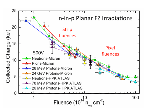
Plot showing the charge collection for different 'n-in-p' sensors and different irradiation sources as a function of fluence up to sLHC levels, with measurements made by different groups. In general the differences are small and, importantly, the performance is predictable.
 Ian Dawson
|